

1. CR
1.1. PSP Photo Stimulus Phosphor
1.1.1. support (base) layer
1.1.2. conductive layer
1.1.3. Phosphor layer
1.1.3.1. barium flourohalide
1.1.3.2. x-ray exposure captured by phosphor atoms
1.1.3.2.1. electrons are caught in traps between valence and conduction band which needs to be "read"
1.1.4. light blocking layer
1.1.5. protective layer
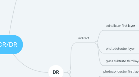
2. DR
2.1. indirect
2.1.1. scintillator first layer
2.1.1.1. exit beam absorbed
2.1.1.2. emits flashes of light in proportion of xray signal
2.1.1.2.1. light spread
2.1.2. photodetector layer
2.1.2.1. amorphous silicon
2.1.2.1.1. generates electric charge proportional to light signal
2.1.3. glass subtrate third layer
2.1.3.1. support surface
2.2. direct
2.2.1. photoconductor first layer
2.2.1.1. amorphous selenium
2.2.2. TFT second layer
2.2.2.1. holds electric charge prior to release to ADC digitization processing and display
2.2.2.2. lower attenuation by selenium needs higher mAs
2.2.2.2.1. no light involved in creating spatial resolution, detection of xray lower than indirect capture
2.3. CCD
2.3.1. silicon matrix
2.3.1.1. highly sensitive to light
2.3.1.1.1. coupled with scintillator to absorb xrays
2.4. CMOS
2.4.1. complementary metal oxide semiconductor
2.4.1.1. scintillation semi conductor