

1. DEFINITION
1.1. IC PACKAGING integrated circuit packaging is the final stage of semiconductor device fabrication, in which the tiny block of semiconducting material is encapsulated in a supporting case that prevents physical damage and corrosion The packaging stage is followed by testing of the integrated circuit.
1.2. IC ASSEMBLY IC assembly is the first processing step after wafer fabrication and singulation that enables ICs to be packaged for systems use. IC assembly is defined as the process of electrically connecting I/O bond pads on the IC to the corresponding bond pads on the package. The package in this case can be a single chip package, a multichip package, or a system level board
2. TYPES
2.1. IC PACKAGING
2.1.1. Through-Hole package
2.1.1.1. Surface Mount Packages
2.1.1.1.1. Contactless Packages
2.2. IC ASSEMBLY
2.2.1. Wirebonding
2.2.1.1. Tape Automated Bonding
2.2.1.1.1. Flip Chip
3. VIDEO
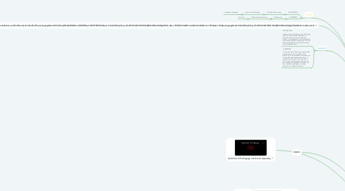
4. Quik-Pak: IC Packaging, Custom IC Assembly
5. IC PACKAGING PROCESS (without wafer backgrind) Front-end
6. https://www.google.com/imgres?imgurl=https%3A%2F%2Fimage.slidesharecdn.com%2Ficpackagingwithoutbackupslides1-13329101975704-phpapp01-120327235211-phpapp01%2F95%2Fic-packaging-6-728.jpg%3Fcb%3D1333531769&imgrefurl=https%3A%2F%2Fwww.slideshare.net%2Fsantoshnimbal%2Fic-packaging&docid=htdG-qLRkHjzhM&tbnid=BZNf4pc1SbWF8M%3A&vet=10ahUKEwjOmp_KhJDYAhUI6Y8KHUHqBbQQMwiXASgCMAI..i&w=728&h=546&hl=en&bih=623&biw=1396&q=ic%20packaging&ved=0ahUKEwjOmp_KhJDYAhUI6Y8KHUHqBbQQMwiXASgCMAI&iact=mrc&uact=8
7. https://www.google.com/imgres?imgurl=https%3A%2F%2Fimage.slidesharecdn.com%2Ficpackagingwithoutbackupslides1-13329101975704-phpapp01-120327235211-phpapp01%2F95%2Fic-packaging-8-728.jpg%3Fcb%3D1333531769&imgrefurl=https%3A%2F%2Fwww.slideshare.net%2Fsantoshnimbal%2Fic-packaging&docid=htdG-qLRkHjzhM&tbnid=sLFbYDOy76M2wM%3A&vet=10ahUKEwjOmp_KhJDYAhUI6Y8KHUHqBbQQMwiVASgAMAA..i&w=728&h=546&hl=en&bih=623&biw=1396&q=ic%20packaging&ved=0ahUKEwjOmp_KhJDYAhUI6Y8KHUHqBbQQMwiVASgAMAA&iact=mrc&uact=8
8. https://www.google.com/url?sa=i&rct=j&q=&esrc=s&source=images&cd=&cad=rja&uact=8&ved=0ahUKEwjF34iTh5DYAhXKgI8KHWzTAj8QjRwIBw&url=http%3A%2F%2Fslideplayer.com%2Fslide%2F5287160%2F&psig=AOvVaw2vaeLYb3VgKX-JIWeM002w&ust=1513566072429951
9. https://www.google.com/url?sa=i&rct=j&q=&esrc=s&source=images&cd=&cad=rja&uact=8&ved=0ahUKEwjE4sSyh5DYAhXBvY8KHQIACL0QjRwIBw&url=https%3A%2F%2Fwww.slideshare.net%2Ffnasir%2Flecture-05-15661363&psig=AOvVaw3yyGjt4NVBZ1Tx25ruKQon&ust=1513566137781089
10. https://www.google.com/url?sa=i&rct=j&q=&esrc=s&source=images&cd=&cad=rja&uact=8&ved=0ahUKEwiHldrOh5DYAhUNTI8KHWOQCx8QjRwIBw&url=https%3A%2F%2Fwww.slideshare.net%2FDeepakFloria%2Fflip-chip-technology&psig=AOvVaw3O4vk2sEQLEVH_1i2hKmDG&ust=1513566185974777
11. ADVANTAGES
11.1. IC PACKAGING
11.1.1. Through-hole packages
11.1.1.1. strong mechanical bonds
11.1.2. Surface Mount packages
11.1.2.1. smaller components
11.1.2.2. fewer holes need to be drilled through abrasive boards.
11.1.3. Chip-Sales packages (CSP)
11.1.3.1. Lower inductance power planes support high frequency
11.1.3.2. supports higher pin counts than wirebond packages
11.1.3.3. improved current distribution providing more ability to minimize IR drops (power is distributed through top metal layer metal bumps.)
12. DISADVANTAGES
12.1. Through-hole packages
12.1.1. additional drilling required makes the boards more expensive to produce
12.2. Surface Mount packages
12.2.1. the process for SMT are much more sophisticated than through-hole boards.
12.2.2. SMDs can't be used directly with breadboards
12.2.3. SMDs' solder connections may be damaged by potting compounds going through thermal cycling.
12.3. Chip-Scale packages (CSP)
12.3.1. -
13. ADVANTAGES
13.1. IC ASSEMBLY
13.1.1. Wirebonding
13.1.1.1. Highly flexible chip-to-package interconnection process
13.1.1.1.1. Low defect rates of high yield interconnection processing
13.1.2. Tape Automated Bonding
13.1.2.1. Ability to handle small bond pads and finer pitches on the IC
13.1.2.1.1. Ability to handle high I/O counts
13.1.3. Flip-Chip
13.1.3.1. Advance form of SMT
13.1.3.1.1. best electrical characteristic
14. DISADVANTAGES
14.1. IC ASSEMBLY
14.1.1. Wirebonding
14.1.1.1. Slower interconnection rates
14.1.1.1.1. long chip-to-packages interconnectio length
14.1.2. Tape Automated Bonding
14.1.2.1. little production infrastructure
14.1.2.1.1. difficulty in assembly rework
14.1.3. Flip Chip
14.1.3.1. process does not have the infrastructure to be mass produced
15. APPLICATION
15.1. IC PACKAGING
15.1.1. National Semiconductor's new micro SMD pakaging enable dramatically smaller printed-circuit boards. because micro SMD packages are smaller than chip capacitors, they look like mere dots on the smaller board.
15.2. ASSEMBLY
15.2.1. Enterprise bean JAR files (known as EJB modules)
15.2.2. Web archive (WAR) files (known as web modules)
15.2.3. Application client JAR files (known as client modules)
15.2.4. Resource adapter archive (RAR) files (known as resource adapter modules
15.2.5. SAR files (known as Session Initiation Protocol (SIP) modules)