
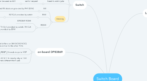
1. Switch
1.1. Understand JTAG requirement
1.1.1. Need to take a look at this, I believe it used only for boundary scan but would like you to take a second look
1.1.1.1. TAP controller access? SPI is used for internal configuration
1.1.1.1.1. TAP and SPI are the same, no need for this on the board
1.2. TRSTN and RSTN need to be held low simultaneously according to datasheet.
1.3. Need to add crystal
1.3.1. sent in request
1.3.1.1. Same crystal as PHY can be used as 869
1.3.1.1.1. used new crystal because ppm needed was 50
1.4. Clocking
1.4.1. MII
1.4.1.1. TX and RX clock are provided by PHY (EVM)
1.4.2. RMII
1.4.2.1. REFCLK provided by switch
1.4.2.1.1. can be generated by the Ethernet switch
1.4.3. RGMII
1.4.3.1. DP83869 RGMII
1.4.3.2. TX CLK provided by switch, RX CLK provided by EVM
2. on-board DP83869
2.1. requires level shifters on SMI (MDIO/MDC) and xMII pins similar to the other PHYs
2.1.1. Level shifters on SMI
2.2. PHY_RESET_N needs to go to MSP
2.3. Check RESET_N circuitry why is EVM schematic different from web
2.3.1. silicon bug, leave it in there can DNP later if needed
3. MSP
3.1. Place SPI series resistors close to source MSP
3.2. Place MDIO/MDC pull-up
3.3. needs ability to turn off SPI signals, either automatically when J6 plugged in or manually
3.3.1. manualy, both will be connected by default but assumption is that the J6 wont be plugged in.
4. SPI Level Shifters
4.1. LSF allows level shifting to constant voltage from any voltage but requires pull-up resistors
4.2. SN74AXC allows level shifting from any provided voltage
4.2.1. Assumption here is that SPI voltage level of the J6 processor is the same as the MDIO and MII levels
4.2.1.1. Make sure processor board takes this into account
4.3. Check back on e2e to see placement of series resistors
4.3.1. https://e2e.ti.com/support/logic/f/151/t/853191
5. Power
5.1. Plug-in EVM power comes from Switch Board
5.1.1. EVM LDOs supply VDDIO_PHYx to level translators
5.1.1.1. This is ok, EVM LDOs designed for 20% margin
6. Level Shifters
6.1. In LSF
6.1.1. MDC doesnt require pull-up on transmitter (MSP) side.
6.1.2. MDC requires pull-up on receiver side when leakage current into the receiver (PHY) is less than 1 uA.
6.1.2.1. How can I check this?
6.1.2.2. Are there any issues with putting a resistor here?
6.1.3. MDIO requires pull-up on PHY side because it is open drain
6.1.4. provides isolation so the MDIO pull-ups are not in parallel on the PHY side
6.1.5. For bidirectional translation pull-ups are always required on the high side and pull-ups are required on the low side if the low side is open drain or has leakage greater than 1 uA
6.1.5.1. MDIO requires pull-ups on both sides
6.1.6. There is a tradeoff between sink current and data rate. For higher datarates sink current is higher, so the PHY and MSP must be able to tolerate this
6.1.6.1. maximum data rate is related to the slow rising edge of the higher voltage side
6.1.6.2. maximum sink current is the sum of the supply voltages divided by their respective pull-up resistors
6.1.6.2.1. Sink current must be tolerated by MDIO / MDC pins on PHY and MSP
6.1.7. When MSP is low driving all the PHYs (down translation) there will be a large sink current
6.1.7.1. 5 * (3.3 V / 2 k-ohm) + (3.3 / MSP pull-up)
6.1.8. When PHY is low driving MSP (up translation) there will be a sink current
6.1.8.1. (3,3 / 2 k-ohm) + (3.3 / MSP pull-up)
6.2. Will two PHYs pulled up to different MDIO voltages communicate with each other? If not and I use 3.3 V for MDI bus voltage for all PHYs is that ok even if their VDDIOs are at a different voltage?
6.2.1. MDIO goes to PHYs and Microcontroller, use 3.3 V for all of these
6.2.2. xMII goes to PHYs and switch use switch requirements for all of these, 2.5 V for RGMII and 3.3 V for MII/RMII
6.2.3. The A voltage and b voltage just need to be two different voltages with a difference > 0.85. Signal voltages can be different
7. Samtek connector Pin out
7.1. TX_CLK/REFCLK on switch is the same pin but needs to go to TX_CLK and XI different pins on the PHY
7.1.1. Need to understand if the SJA1105 allows the PHY to be in master mode, if so need another pin on the connector for 50 MHz from PHY considering that this comes from different pins on different PHYS
7.1.1.1. phy boards need to output REFCLK, MAC MAC mode can be used to use PHY in master
7.2. port4 has a jumper to connect disconnect the power to the connected board, while the other ports have a 0-ohm
7.2.1. 0-ohms can take 1.5 W
7.3. CRS, COL and INH go to header
7.4. WAKE, PDN and RESET go to MSP gpio
7.5. switch SPI interface can operate at 3.3, 2.5 or 1.8 determined by the voltage connected to VDDIO_HOST
7.5.1. decided to use 3.3 V on SPI interface
7.6. Needs cutout
8. TODO
8.1. Things to do at the end
8.1.1. Not Fitted Components
8.1.1.1. DNP all MDIO/MDC pull-ups on level shifters PHY side
8.1.1.2. PTP Clock SMA, DNP?
8.1.1.3. DNP 0-hm resistors on level shifter signals that are needed for RMII set default to not RMII
8.1.2. Check shunt and header #s match